


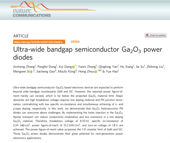
半导体产业网讯:从西安电子科技大学微电子学院官网获悉,近期,西安电子科技大学郝跃院士团队张进成教授、周弘教授等在超宽禁带半导体氧化镓功率器件研究方面取得重要进展,研制出一种新型的空穴超注入p-NiO/n-Ga2O3半导体异质结二极管。该结构通过异质结空穴超注入效应,实现了兼具超高耐压和极低导通电阻的氧化镓功率二极管,功率优值高达13.2GW/cm2,是截止目前氧化镓半导体器件的最高值。
相关成果以《Ultra-wide bandgap semiconductor Ga2O3power diodes》为题发表于国际期刊《自然·通讯》(Nature Communications)。
研究背景
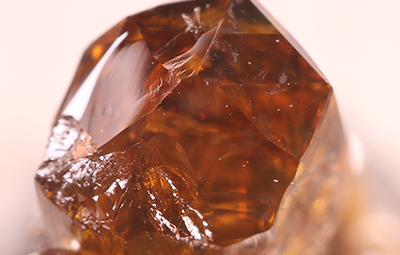
氧化镓(β-Ga2O3)是超宽禁带半导体的典型代表,禁带宽度高达(~4.8 eV),临界击穿场强高达(~8 MV/cm),是研制高耐压、大功率和高效节能半导体器件的理想半导体材料之一,可实现高击穿、低功耗和低成本器件芯片三重优势,在电力传输转换、电动汽车、高铁等领域具有重大应用前景。与当前产业界火热的第三代半导体GaN和SiC相比,Ga2O3功率器件在相同耐压情况下具有更低的导通电阻,应用于电能转换领域将实现更低的功耗和更高的转换效率。因此,近年来,氧化镓半导体已成为半导体国际研究热点和大国技术竞争制高点。2018年以来,在郝跃院士领导下,西安电子科技大学通过自主氧化镓生长MOCVD设备、高质量氧化镓外延材料、高压器件新结构与新工艺等一系列技术创新,实现了氧化镓功率二极管和功率晶体管性能的高速提升,如图1和2,取得了多项里程碑成果,使我国氧化镓功率器件研究水平进入国际前列。
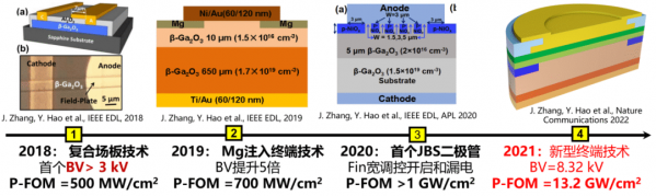
图1 西安电子科技大学氧化镓功率二极管研究进展

图2 西安电子科技大学氧化镓功率晶体管研究进展
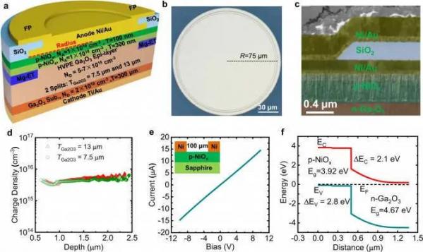
Fig. 1 UWB power diodes design and implementation. a 3-D cross-sectional schematic of the Ga2O3 power diodes with HJ architecture and composite electric field management. b Top view of a fabricated Ga2O3 power diode. c False-colored SEM image of the cross-sectional anode field plate region with p-NiOx thickness of 400 nm. d Extracted carrier concentration of two representative samples with concentration of 5 × 10¹⁵−7 × 1015 cm−3. e Currentvoltage behavior of the Ni pads on p-NiOx with NA = 1019 cm−3, showing an Ohmic contact. f Simulated band diagram of the p-NiOx/n-Ga2O3 HJ structure. The band bending occurs in n-Ga2O3 and the conduction band offset is only 2.1 eV, showing the great promise of low Von even for a UWB material.
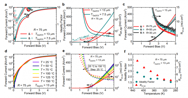
Fig. 2 UWB Ga2O3 power diodes forward characteristics. a Forward current-voltage-ideality factor characteristics of two Ga2O3 power diodes with TGa2O3 = 7.5 and 13 μm. b Forward current–voltage-specific on-resistance Ron,sp characteristics of the same diodes as a. A decent Von = 1.8 V with minimal Diff. Ron,sp = 2.9 and 5.24 mΩ cm2 as well as extracted overall Ron,sp (@VF = 3 V) of 15.3 and 29.5 mΩ cm2 for TGa2O3 = 7.5 and 13 μm are achieved. c Radius-dependent forward current-voltage-resistance curves for diodes with TGa2O3 = 13 μm. T-dependent d log-scale and e linear-scale forward characteristics of diode with TGa2O3 = 13 μm. On/Off ratio of 1010 and 108 are achieved for T = 25 °C and 150 °C, respectively. At all temperatures, Ron,sp drops when VF increases, verifying the conductivity modulation effect. f Extracted T-dependent ideality factor and Ron,sp values as e.
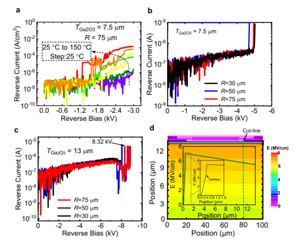
Fig. 3 UWB Ga2O3 power diodes with high breakdown voltages. a T-dependent reverse current–voltage characteristics of diode with TGa2O3 = 7.5 μm. With increased T, IR increases, indicating a non-avalanche breakdown. Room temperature reverse current–voltage characteristics of diodes with TGa2O3 = 7.5 μm (b) and 13 μm (c) at various radiuses. A BV of 5.1 kV and 8.32 kV are achieved for diodes with TGa2O3 = 7.5 and 13 μm, yielding an averaged E of 6.45 MV/cm and 6.2 MV/cm, respectively. d Simulated E distribution of the diode with BV = 8.32 kV and TGa2O3 = 13 μm. Due to the small ND = 6 × 1015 cm−3, a fully depletion and a small E slope of the drift layer is observed.
研究创新
由于p型掺杂困难,空穴迁移率低,氧化镓功率器件中载流子双极输运及其电导调制效应始终没有实现,这是制约氧化镓功率器件性能进一步提升的关键瓶颈。
为此,本文构筑了一种新型p-NiO/n-Ga2O3异质型PN结二极管结构。一方面,通过将PN异质结、镁注入终端、高k/低k泊松终端场板等相复合,利用高温热退火抑制非故意掺杂,使器件峰值电场强度得到极大的削弱;为高耐压氧化镓器件发展开拓了新技术途径,实现了8.3 kV的超高耐压。
另一方面,得益于低导带带阶PN异质结的设计,超宽禁带PN异质结功率二极管实现了较低的开启,正向偏置时,空穴势垒降低,p区空穴跃过PN异质结进入n区,当空穴浓度高于电子浓度后,诱导电子浓度上升,从而显著降低了器件导通电阻,随着正向电压的增加微分电阻持续降低,在氧化镓器件中实现了空穴超注入效应。研制的氧化镓功率二极管拥有超高耐压和极低电阻,功率优值P-FOM高达13.2 GW/cm2,是截止目前氧化镓半导体器件的最高值。
论文原文链接:https://www.nature.com/articles/s41467-022-31664-y.pdf
来源:西安电子科技大学微电子学院
原文转载于公众号【第三代半导体产业】