


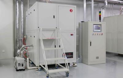


世界各国为生长大尺寸氮化铝单晶,近50年来在晶体生长方法、生长工艺等方面作出了长期不懈努力,但研发进展非常缓慢。其中,物理气相沉积法被公认为生长块状氮化铝单晶的唯一方法,该方法也是生长大尺寸块状碳化硅单晶理想方法。尽管氮化铝单晶和碳化硅单晶生长的基础研究同时起步于20世纪70年代,而碳化硅单晶生长工艺进展迅速,目前国际上已成功研发并计划量产直径8英寸(200mm)碳化硅晶圆,但当前国际上有能力生长出直径1英寸(25.4mm)氮化铝单晶的科研机构及企业极其有限。由于氮化铝单晶生长温度高、生长条件非常苛刻,对氮化铝单晶生长的设备、热场及其控制系统提出了前所未有的挑战。因此,国务院、国家工信部将氮化铝单晶生长装备列入《中国制造2025》绿皮书有待突破的关键国产化装备......
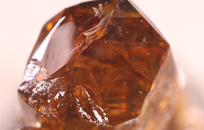
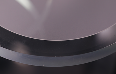
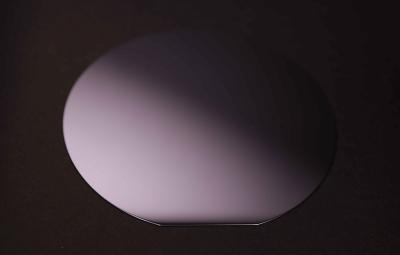
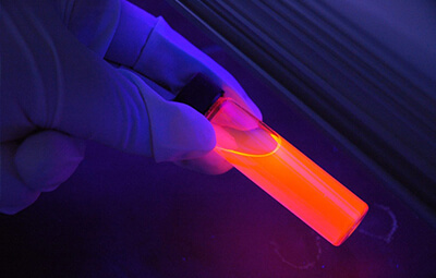
应诺贝尔物理奖获得者天野浩教授为会议主席的组委会邀请,奥趋光电技术( 杭州) 有限公司在日本横滨4月23-25 日举行的LED 工业应用国际会议( LEDIA-2019) 上,推出了直径60 mm 氮化铝单晶及晶圆,该晶圆为迄今为止国内外见诸报道的最大尺寸氮化铝晶圆。检测结果表明,晶片的拉曼半高宽仅为2.85cm-1,深紫外260-280 nm 波段下的吸收系数低至14-21 cm-1,关键性能指标居全球领先水平。相关成果发表在权威学术期刊《Physica Status Solidi A》上,并作为该期刊封面进行了特别展示。该成果标志着中国在第三/四代半导体关键战略新材料氮化铝单晶领域取得突破性进展,在此之前,美国在全球氮化铝单晶及晶圆制造方面直径最大可达2英寸(50.8 mm),长期处于技术垄断地位......
传统硅基等半导体材料已经无法满足当前电子器件的发展要求。氮化铝作为第三代/第四代半导体材料的典型代表,具有超宽禁带、高热导率、高击穿场强、高电子迁移率、耐腐蚀、耐辐射等优越物理化学性能,特别适合于制造射频通信器件、光电子器件、电力电子器件等,是紫外LED、紫外探测器、紫外激光、高功率/高频电子器件等最佳衬底材料,广泛应用于环保、电子、无线通讯、印刷、生物、医疗、军事等领域,如紫外净化/灭菌(污水处理、饮用水消毒、空气杀菌、表面杀菌、除臭等)、紫外固化、紫外催化、5G无线通信 SAW/BAW等器件、防伪检测、高密度存储、医学光照治疗、药物研发及保密通信、紫外空间探测等领域......
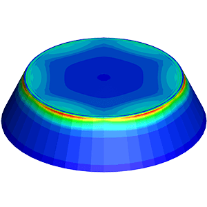
通常,PVT法生长氮化铝单晶生长温度高达2000ºC - 2300ºC,且晶体生长在密闭环境下进行,单晶生长周期长、对温度场的稳定性及其控制系统精度提出了前所未有的挑战。由于氮化铝单晶生长温度高、生长条件非常苛刻,通过实际实验来调整工艺参数获取有限的实验数据极其困难且成本高昂,或具备不具备可行性。因此,利用数值模拟仿真手段,开展AlN晶体生长过程的仿真研究已成为分析、优化晶体生长过程不可或缺的工具......